ioTech – io600
The electronics industry is facing challenges in semiconductor packaging, with a demand for smaller and more flexible components. Manufacturers aim to increase chip production per wafer, enhance data transfer speeds, and reduce the size of components like gaskets and microphones. However, existing packaging methods based on subtractive technologies – – etching and electroplating – are environmentally harmful, labor-intensive, and reaching resolution limits in their current forms.
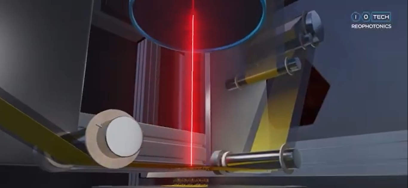
ioTech‘s io600 offers a breakthrough by leveraging its patented Continuous Laser-Assisted Deposition (CLAD) process, allowing precise and fast deposition of materials. The io600 handles a wide range of materials with high accuracy (30 μm resolution) and high throughput (over 5 million drops per hour). It reduces the need for extensive cleanroom space and lowers labor costs due to its automation.
The technology involves coating materials on a foil and using a pulse laser for precise jetting, followed by necessary post-processing. This method ensures accurate, contactless deposition on various substrates, leading to higher yields and finer feature resolutions while following a process without employing polluting materials as subtractive techniques do.
Recognizing the industry’s need for cutting-edge solutions, the EIC provided funding for Iotech’s project through its program in March 2024. They received blended finance with 2.5 Million in grant and 10 million in equity.
Iotech’s technology supports the industry’s shift towards more powerful chips and aligns with environmental and digital transitions. In this regard, Iotech contributes to the EU Chips Act as it enables the miniaturization of chips and the reshoring of their production from Asia to Europe.

